Not for rocketry, but still cool electronics

The Rocketry Forum

Help Support The Rocketry Forum:

This site may earn a commission from merchant affiliate links, including eBay, Amazon, and others.
Computer History at Lawrence Livermore National Laboratory 1950-1983 - UNIVAC LARC, IBM, CDC, CRAY

Cray XMP "supercomputer" at LLNL in 1983:

Clock: 117 MHz
Memory: 250 megabits
Power use: 300 kilowatts
942 MegaFLOPS
Cost: $15 million in 1984 dollars ($37 million in 2018 dollars)

AMD Ryzen 7 2700X in 2018:

Clock: 3,700 to 4,300 MHz
Power use: 65 watts
127.79 GigaFLOPS (127,790 MegaFLOPS)
Cost: $320

This 1983 film created by Lawrence Livermore National Laboratory (“LLNL”), gives a fascinating and concise history of its computer developments both as a purchaser of early computers and a co-designer of many early technologies, from the early 1950’s up to 1983 (where the film ends). The Lab continues to be a leader in science in technology today. This film has been slightly restored and enhanced to improve view ability. Narrator, Dr. John Fletcher, provides a fascinating chronological walk through historical implementations of computing technology, especially with regard to Livermore’s role in computer design, and the establishment of its “Octopus” computer network. Highly recommended viewing for anyone interested in computer history. Uploaded by Mark Greenia, for the Computer History Archive Project.

Computers mentioned include: UNIVAC 1, Univac LARC, IBM 7030, IBM 7090 & 7094, CDC 1604, CDC 3600, CDC 6600, Cray XMP and many others.
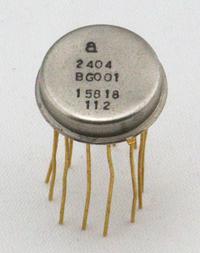
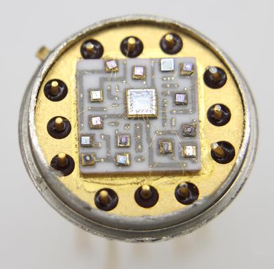
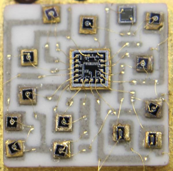
 
If you've ever considered restoring old electronic gear, watch this guy's channel! His beautifully done videos are absolutely packed with very important info gleaned from his long experience doing just that.

 
World's first commercial, electronic (tubes & germanium diodes), digital, stored-program computer. Clock - 4 MHz later reduced to 2.5 MHz for greater reliability.

BINAC: Binary Automatic Computer (1948)

 
Looking inside a $1.3 MILLION o'scope - what the guts of the most advanced o'scope ever made looks like (amazing).

Keysight Technologies, or Keysight, is a US company that manufactures electronics test and measurement equipment and software. In 2014, Keysight was spun off from Agilent Technologies, taking with it the product lines focused on electronics and radio, leaving Agilent with the chemical and bio-analytical products.

The Keysight UXR-Series Real-Time Oscilloscope brings 110GHz of analog bandwidth and 256GS/s real-time sampling at 4-channels simultaneously. To make it even more impressive, the entire data-conversion architecture is in 10-bits. This implies that the instruments captures, processes, stores and displays over 10Tb/s of information.

Various architectures of state-of-the art oscilloscopes from Keysight, LeCroy and Tektronix are examined and compared against the new real-time architecture of the UXR-Series oscilloscope. The teardown of the front-end 110GHz module along with the data acquisition board is presented and analyzed in detail. The instrument showcases a wide range of Keysight technologies implemented in various technologies such as InP, SiGe BiCMOS, 65nm CMOS and 28nm CMOS nodes. In combination with Hyper-Cube memory module, data can be captured at 256GS/S from all 4-channels at the same time. Several variants of the UXR-Series oscilloscope will be available from 13GHz to 110GHz bandwidths.

A new calibration probe is also introduced based on the Keysight InP process capable of producing signal edges with sub-3.5ps of rise/fall times with NIST traceable calibration data. This enables users to perform NIST alignment and bandwidth calibration on site without needing to send the instrument back to Keysight.

Several measurements with the scope demonstrates its extraordinarily low noise floor, jitter as well as the capability of the new probe module for instrument calibration. The 110GHz 4-channel variant of the UXR-Series oscilloscope has an MSRP of $1.3 Million US dollars.


Commodore 64 left outside for over a decade! Could it still work?

 
That's pretty amazing. We don't have any more 8-bit Commodore stuff but I remember them fondly. I wrote some of my first published articles on a C-64.
 
That's pretty amazing. We don't have any more 8-bit Commodore stuff but I remember them fondly. I wrote some of my first published articles on a C-64.
The restoral. To skip too long C64 musical intro, start at 3:06:

 
I happened to see today one of these for sale on eBay while looking for PDP stuff and remembered the one I still own and photographed externally and internally. For about a six month period back when no one had previously done this sort of thing, to preserve their great beauty I bought, opened and photographed as many interesting computer and computer support ICs available at reasonable prices as I could find. Huge lots of classic computer chips at that time were very widely being ground up wholesale for their gold content.

My DEC DCJ-11 chipset on its ceramic carrier:

44732466504_eb2d494405_o.jpg


The DEC DCJ-11 chipset was introduced 1983 and cost around $450 ($1,115 in 2018 dollars). It was supposedly used in the DEC PDP-11/53, 11/73, 11/83, and 11/84.

Its innards:

Control Unit

45457510021_ed50756200_o.jpg


The Control Unit implements the micro word access and sequencing functions of the J-11 chipset. Key features were:
ROM/PLA control store (512 x 25 bit PLA terms, 768 ROM terms)

Chipset micro sequencer
Next address logic
Micro subroutine stack
Interrupt logic
Abort logic
Initial decode PLA (Q logic)
External interface sequencer
Instruction prefetching logic

Data Unit

44732466914_cb4049eb90_o.jpg


The Data Unit implemented the instruction execution and memory management data paths of the chipset. It shares the responsibility for the external interface and for instruction prefetching with the Control Unit. The Data Unit operates under the control of micro words fetched from the Control Unit. Its key features were:

Execution unit
PDP-11 architectural general registers (16 bit): dual register set, three stack pointers
Processor status word (PSW)
Microcode temporary registers (32 bit)
Full function arithmetic/logic unit (32 bit)
Single bit shifter
Byte swapper
Conditional branch logic
Memory management unit
PDP-11 memory management registers: kernel, supervisor, user; instruction and data spaces
Address translation logic (22 bit)
Protection logic
External interface sequencer
Instruction prefetching logic

The list of what I opened and photographed:

45457509121_ac872c0e20_o.jpg


Just a few of the photos I took:

https://diephotos.blogspot.com/
 
Still have a 68000 :) Don't know if it still works, don't have the support circuitry.M68000a.jpg

M68000b.jpg
 
I still have a couple of 68000-based computers that still work. One of them I designed from scratch in the 1980's. Time flies when you're having fun. ;-)
 
Incredibly cool. HD demonstration video of completed system.

Some stats:

Number of transistors: 42,400
Number of resistors: 50,500
Number of LEDs: 10,500
Number of 20 & 30 way IDC connectors: 770
Number of single pin terminals: 7,700
Number of solder joints: 272,300
Weight of solder: 4.25Kg
Length of single conductor wire: ~1,500m
Length of 20 conductor ribbon: 420m
Aggregate length of cable conductors: 9.9 km

 
New Metal-Air Transistor Replaces Semiconductors
A novel field emission transistor that uses air gaps could breathe life into Moore’s Law
30 Nov 2018

https://spectrum.ieee.org/nanoclast...w-metalair-transistor-replaces-semiconductors

It is widely predicted that the doubling of silicon transistors per unit area every two years will come to an end around 2025 as the technology reaches its physical limits. But researchers at RMIT University in Melbourne, Australia, believe a metal-based field emission air channel transistor (ACT) they have developed could maintain transistor doubling for another two decades.

The ACT device eliminates the need for semiconductors. Instead, it uses two in-plane symmetric metal electrodes (source and drain) separated by an air gap of less than 35 nanometers, and a bottom metal gate to tune the field emission. The nanoscale air gap is less than the mean-free path of electrons in air, hence electrons can travel through air under room temperature without scattering.

“Unlike conventional transistors that have to sit in silicon bulk, our device is a bottom-to-top fabrication approach starting with a substrate. This enables us to build fully 3D transistor networks, if we can define optimum air gaps,” says Shruti Nirantar, lead author of a paper on the new transistor published this month in Nano Letters. “This means we can stop pursuing miniaturization, and instead focus on compact 3D architecture, allowing more transistors per unit volume.”

Using metal and air in place of semiconductors for the main components of the transistor has a number of other advantages, says Nirantar, a Ph.D. candidate in RMIT’s Functional Materials and Microsystems Research Group. Fabrication becomes essentially a single-step process of laying down the emitter and collector and defining the air gap. And though standard silicon fabrication processes are employed in producing ACTs, the number of processing steps are far fewer, given that doping, thermal processing, oxidation, and silicide formation are unnecessary. Consequently, production costs should be cut significantly.

In addition, replacing silicon with metal means these ACT devices can be fabricated on any dielectric surface, provided the underlying substrate allows effective modulation of emission current from source to drain with a bottom-gate field.

“Devices can be built on ultrathin glass, plastics, and elastomers,” says Nirantar. “So they could be used in flexible and wearable technologies.”
Replacing the solid-channel transistors in space circuitry is another potential application. Because the electrons flow between the electrodes just as well in a vacuum (think vacuum tube) as in air, radiation will not modulate channel properties, making ACT devices suitable for use in extreme radiation environments and space.

Now that the researchers have proof of concept, the next step is to enhance stability and improve component efficiency by testing different source and drain configurations and using more tolerant materials. In fabricating the prototype ACTs, the researchers used electron-beam lithography and thin-film deposition, while tungsten, gold, and platinum were evaluated as metals of choice.

“We also need to optimize the operating voltage as the electrode metal tips are experiencing localized melting due to concentrated electric fields,” notes Nirantar. “This decreases their sharpness and emission efficiency. So we’re looking at designs that will increase collector efficiency to decrease stress on the emitter.” She believes this can be accomplished over the next two years.

Looking further ahead, she points out that the theoretical speed of an ACT is in the terahertz range, some 10 thousand times as fast as the speed at which current semiconductor devices work. “So further research is needed to find and demonstrate the operational limits,” she adds.
As for commercialization, Nirantar says access to industrial fabrication facilities and support from industry to scale up to 3D networks of the transistors will be necessary. “With such help and sufficient research funding, there is the potential to develop commercial-grade field emission air-channel transistors within the next decade—and that’s a generous timeline. With the right partners, this could happen more quickly.”


MzE4MTkyNA.jpeg
 
Incredible...

On the Origin of Circuits

https://www.damninteresting.com/on-the-origin-of-circuits/

Excerpts:

In a unique laboratory in Sussex, England, a computer carefully scrutinized every member of large and diverse set of candidates. Each was evaluated dispassionately, and assigned a numeric score according to a strict set of criteria. This machine’s task was to single out the best possible pairings from the group, then force the selected couples to mate so that it might extract the resulting offspring and repeat the process with the following generation. As predicted, with each breeding cycle the offspring evolved slightly, nudging the population incrementally closer to the computer’s pre-programmed definition of the perfect individual.

The candidates in question were not the stuff of blood, guts, and chromosomes that are normally associated with evolution, rather they were clumps of ones and zeros residing within a specialized computer chip. As these primitive bodies of data bumped together in their silicon logic cells, Adrian Thompson— the machine’s master— observed with curiosity and enthusiasm.

Dr. Adrian Thompson is a researcher operating from the Department of Informatics at the University of Sussex, and his experimentation in the mid-1990s represented some of science’s first practical attempts to penetrate the virgin domain of hardware evolution. The concept is roughly analogous to Charles Darwin’s elegant principle of natural selection, which describes how individuals with the most advantageous traits are more likely to survive and reproduce. This process tends to preserve favorable characteristics by passing them to the survivors’ descendants, while simultaneously suppressing the spread of less-useful traits.

Dr. Thompson dabbled with computer circuits in order to determine whether survival-of-the-fittest principles might provide hints for improved microchip designs. As a test bed, he procured a special type of chip called a Field-Programmable Gate Array (FPGA) whose internal logic can be completely rewritten as opposed to the fixed design of normal chips. This flexibility results in a circuit whose operation is hot and slow compared to conventional counterparts, but it allows a single chip to become a modem, a voice-recognition unit, an audio processor, or just about any other computer component. All one must do is load the appropriate configuration.

For the first hundred generations or so, there were few indications that the circuit-spawn were any improvement over their random-blob ancestors. But soon the chip began to show some encouraging twitches. By generation #220 the FPGA was essentially mimicking the input it received, a reaction which was a far cry from the desired result but evidence of progress nonetheless. The chip’s performance improved in minuscule increments as the non-stop electronic orgy produced a parade of increasingly competent offspring. Around generation #650, the chip had developed some sensitivity to the 1kHz waveform, and by generation #1,400 its success rate in identifying either tone had increased to more than 50%.

Finally, after just over 4,000 generations, test system settled upon the best program. When Dr. Thompson played the 1kHz tone, the microchip unfailingly reacted by decreasing its power output to zero volts. When he played the 10kHz tone, the output jumped up to five volts. He pushed the chip even farther by requiring it to react to vocal “stop” and “go” commands, a task it met with a few hundred more generations of evolution. As predicted, the principle of natural selection could successfully produce specialized circuits using a fraction of the resources a human would have required. And no one had the foggiest notion how it worked.

Dr. Thompson peered inside his perfect offspring to gain insight into its methods, but what he found inside was baffling. The plucky chip was utilizing only thirty-seven of its one hundred logic gates, and most of them were arranged in a curious collection of feedback loops. Five individual logic cells were functionally disconnected from the rest— with no pathways that would allow them to influence the output— yet when the researcher disabled any one of them the chip lost its ability to discriminate the tones. Furthermore, the final program did not work reliably when it was loaded onto other FPGAs of the same type.

It seems that evolution had not merely selected the best code for the task, it had also advocated those programs which took advantage of the electromagnetic quirks of that specific microchip environment. The five separate logic cells were clearly crucial to the chip’s operation, but they were interacting with the main circuitry through some unorthodox method— most likely via the subtle magnetic fields that are created when electrons flow through circuitry, an effect known as magnetic flux. There was also evidence that the circuit was not relying solely on the transistors’ absolute ON and OFF positions like a typical chip; it was capitalizing upon analogue shades of gray along with the digital black and white.
 
Vision-Based High Speed Driving with a Deep Dynamic Observer

https://arxiv.org/pdf/1812.02071.pdf

In order to test the performance of these algorithms in a real racing scenario, we utilize the AutoRally [3] platform. This robot is based on a 1:5 scale RC chassis capable of speeds of nearly 60mph. It has a desktop-class Intel i7 processor and NVidia Gtx 1050 GPU for processing. IMU, GPS, and wheel speed sensors are used, as well as images
captured from an on-board Point Grey camera. This allows all computation to be performed in real time on-board the vehicle. All software runs under the Robot Operating System ROS). Particle filter and MPPI code is written in CUDA, and CNN forward inference is done using a custom ROS wrapper around TensorFlow.


Not electronics, but coding... and amazing:

A Single Cell Hints at a Solution to the Biggest Problem in Computer Science
One small amoeba found a solution to the traveling salesman problem faster than our best algorithms. What does it know that we don't?
27 Dec 2018

https://www.popularmechanics.com/science/math/a25686417/amoeba-math/

One of the oldest problems in computer science was just solved by a single cell.

A group of researchers from Tokyo’s Keio University set out to use an amoeba to solve the Traveling Salesman Problem, a famous problem in computer science. The problem works like this: imagine you’re a traveling salesman flying from city to city selling your wares. You’re concerned about maximizing your efficiency to make as much money as possible, so you want to find the shortest path that will let you hit every city on your route.

There’s no simple mathematical formula to find the most efficient route for our salesman. Instead, the only way to solve the problem is to calculate the length of each route and see which one is the shortest.

What’s worse, performing this calculation gets exponentially harder the more cities are added to the route. With four cities, there are only three different routes to consider. But with six cities, there are 360 different routes that need to be calculated. If you’ve got a route with ten or more cities the number of possible routes is in the millions.
This makes the traveling salesman problem one of a broad class of problems computer scientists call ‘NP hard.’ These are problems that get exponentially difficult very quickly, which also includes problems related to hacking encrypted systems and cryptocurrency mining. For pretty obvious reasons, a lot of people are interested in finding ways to solve these problems as quickly as possible.

Keio University's solution is different from the typical algorithmic solutions produced by other researchers, because the scientists used an amoeba. Specifically, the Physarum polycephalum slime mold. Physarum polycephalum is a very simple organism that does two things: it moves toward food and it moves away from light. Millions of years of evolution has made Physarum abnormally efficient at both of these things.

The Keio University researchers used this efficiency to build a device to solve the traveling salesman problem. They set the amoeba in a special chamber filled with channels, and at the end of each channel the researchers placed some food. Instinctively, the amoeba would extend tendrils into the channels to try and get the food. When it does that, however, it triggers lights to go off in other channels.

In this particular case, each channel represents a city on our hypothetical salesman’s route, along with the order that city should be visited. When the amoeba extends into a channel representing a city, it affects the likelihood that a light will go off in channels representing the next cities on the route. The farther away that city is, the more frequently the light will go off in that channel.

This might seem like a roundabout way of calculating the solution to the traveling salesman problem, but the advantage is that the amoeba doesn’t have to calculate every individual path like most computer algorithms do. Instead, the amoeba just reacts passively to the conditions and figures out the best possible arrangement by itself. What this means is that for the amoeba, adding more cities doesn’t increase the amount of time it takes to solve the problem.

So the amoeba can solve an NP-hard problem faster than any of our computer algorithms. How does this happen? The Keio scientists aren’t sure, exactly.

“The mechanism by which the amoeba maintains the quality of the approximate solution, that is, the short route length, remains a mystery,” says lead study author Masashi Aono in a press release.

But if the researchers can figure out just how the amoeba works, they can use this trick for more than just helping out traveling salesmen. It could speed up our ability to solve all kinds of difficult computational problems and change the way we approach security.

This one small amoeba—and the way it solves difficult problems—might just change the face of computing forever.
 
An impressive example of using cheap modules carrying numerous SMD components to nearly eliminate SMD soldering on a PCB motherboard, and thereby doing impressive things at very low cost and with minimal kit assembly effort. I think anyone designing DIY electronics for rocketry should do the same whenever possible.

 
An impressive example of using cheap modules carrying numerous SMD components to nearly eliminate SMD soldering on a PCB motherboard, and thereby doing impressive things at very low cost and with minimal kit assembly effort. I think anyone designing DIY electronics for rocketry should do the same whenever possible.


Given the difficulty involved in home soldering SMD's I absolutely agree. I have enough trouble these days keeping my hands steady to solder point-to-point or on thru-hole boards with 0.100 pitch! I have a multifunction timer kit stashed away that I seriously doubt I could build now.
 
I’ve built a half dozen flight computers using off the shelf modules like this. I’ll put up a post eventually with pictures and plans. They work great for logging and deployment - even guidance or airstarts. Total cost is less than a G class reload. The penalty is size of course, but you can cram a lot onto a small prototype board if you’re creative...

Some of the newer IOT Microcontrollers like the ESP32 give you so much more to work with these days and they’re dirt cheap (especially if you order direct and in bulk from China). My latest incarnation even has a web browser interface with pretty graphs and an optional plug in display. Because why not...

The time consuming part is the software. I’ve open sourced all of mine but it’s a continual work in progress.
 
I am a mite rusty on embedded coding but I go way back to the days of assembler code on a 16-bit computer with only 16 registers and no memory protection. Might be able to help out on the software side...I also did a lot of C programming 'back in the day.'
 
I’ve built a half dozen flight computers using off the shelf modules like this. I’ll put up a post eventually with pictures and plans. They work great for logging and deployment - even guidance or airstarts. Total cost is less than a G class reload. The penalty is size of course, but you can cram a lot onto a small prototype board if you’re creative...

Some of the newer IOT Microcontrollers like the ESP32 give you so much more to work with these days and they’re dirt cheap (especially if you order direct and in bulk from China). My latest incarnation even has a web browser interface with pretty graphs and an optional plug in display. Because why not...

The time consuming part is the software. I’ve open sourced all of mine but it’s a continual work in progress.
Fantastic!!! Really looking forward to seeing that.

My idea for a future effort on my part is to test the feasibility of using two 915MHz LoRa modules associated with two 3.3V Arduino Pro Minis, a barometric sensor module in the flight hardware, and a tape measure element 915MHz DIY handheld yagi on the ground to produce an RSSI reading RDF system with a variable, metal detector style audio tone for RDF and an LCD altitude readout, all of the very low mass ground hardware being mounted on the yagi handle. As is always the case for me, the component choices were made based upon an absolute minimum cost goal, not because I must, but because I like doing that.

EDIT: Ha! On the idea mentioned above which I just started researching yesterday, I did a search on the unlikely possibility of doing some kind of ranging with the SX1276 LoRa module and found an apparently fairly new 2.4GHz LoRa module specifically made for ranging but still providing data transfer capability, the SX1280:

How to Perform Ranging Tests with the SX1280 Development Kit

https://www.semtech.com/uploads/documents/AN1200.31_SX1280_EVK_Ranging_How_To_V1.0.pdf

From that:

"Although SX1280 can provide reliable ranging results in excess of 7 km"

Data sheet:

SX1280/SX1281
Long Range, Low Power, 2.4 GHz Transceiver with Ranging Capability


https://www.semtech.com/uploads/documents/DS_SX1280-1_V2.2.pdf

And cheap modules are available on eBay:

https://www.ebay.com/sch/i.html?_from=R40&_trksid=m570.l1313&_nkw=SX1280+module&_sacat=0

However, I suspect the 2.4GHz frequency won't be as easily received as the 915MHz frequency once a rocket E-bay reaches the ground, assuming that even the 915MHz frequency will be receivable, the potential Achilles heal for the entire idea.
 
Last edited:
However, I suspect the 2.4GHz frequency won't be as easily received as the 915MHz frequency once a rocket E-bay reaches the ground, assuming that even the 915MHz frequency will be receivable, the potential Achilles heal for the entire idea.
However, however, since this is intended to be a cheap, stand-alone (no GPS mapping capability needed) loss of track prevention device, as long as the rocket link is acquired while still airborne, tracking after landing isn't as critical.
 
I'd NEVER have guessed this would happen:

Running LEDs in reverse could cool future computers
February 13, 2019

https://phys.org/news/2019-02-reverse-cool-future.html

"The LED, with this reverse bias trick, behaves as if it were at a lower temperature," Reddy said.

To get enough infrared light to flow from an object into the LED, the two would have to be extremely close together—less than a single wavelength of infrared light. This is necessary to take advantage of "near field" or "evanescent coupling" effects, which enable more infrared photons, or particles of light, to cross from the object to be cooled into the LED.

The group proved the principle by building a minuscule calorimeter, which is a device that measures changes in energy, and putting it next to a tiny LED about the size of a grain of rice. These two were constantly emitting and receiving thermal photons from each other and elsewhere in their environments.

"Any object that is at room temperature is emitting light. A night vision camera is basically capturing the infrared light that is coming from a warm body," Meyhofer said.

But once the LED is reverse biased, it began acting as a very low temperature object, absorbing photons from the calorimeter. At the same time, the gap prevents heat from traveling back into the calorimeter via conduction, resulting in a cooling effect.

The team demonstrated cooling of 6 watts per meter squared. Theoretically, this effect could produce cooling equivalent to 1,000 watts per meter squared, or about the power of sunshine on Earth's surface.
 
Op amp on the Moon: Reverse-engineering a hybrid op amp module

https://www.righto.com/2019/02/op-amp-on-moon-reverse-engineering.html

The story (here and here) is that during his visit Bob Pease got in a discussion with some Amelco engineers about NASA's requirements for a new low-power, low-noise amplifier. Bob Pease proceeded to design an op amp during his coffee break that met NASA's stringent requirements. This op amp was used in a seismic probe that Apollo 12 left on the Moon in 1969, so there's one of these op amps on the Moon now. Amelco marketed this op amp as the 2401BG.

As for the 2404BG I disassembled, its circuitry is very similar to Bob Pease's 2401BG design5, so I suspect he designed both parts. The 2404BG op amp also made it to the Moon; it was used in the high voltage power supply of the Lunar Atmosphere Composition Experiment (LACE). LACE was a mass spectrometer left on the Moon by the Apollo 17 mission in 1972. (LACE determined that even though the moon has almost no atmosphere, it does has some helium, argon, and possibly neon, ammonia, methane and carbon dioxide.)


bg001-w200.jpg

can-opened-w400.jpg

chip-w600.jpg
 
Fully Levitating Magnetic EZ-Spin Motor - Pyrolytic Graphite

 
Back
Top