Not for rocketry, but still cool electronics

The Rocketry Forum

Help Support The Rocketry Forum:

This site may earn a commission from merchant affiliate links, including eBay, Amazon, and others.
RESTORING THE HEATHKIT ES-400 COMPUTER

https://www.nutsvolts.com/magazine/article/restoring-the-heathkit-es-400-computer

Excerpts:

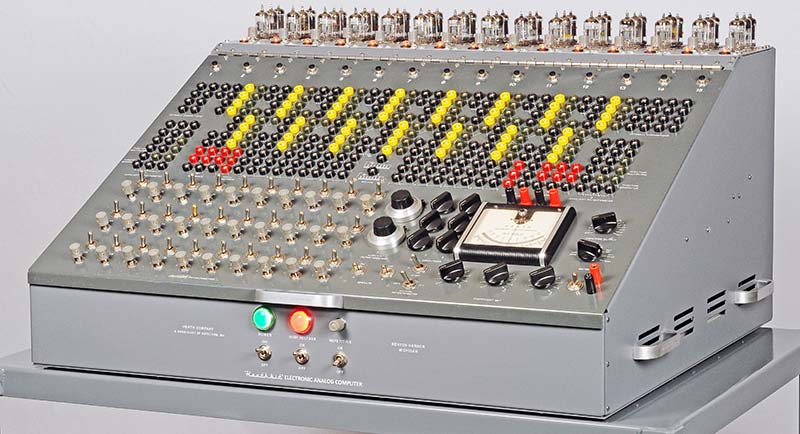
When I first got into electronics in the mid-1950s, I would pour over the Heathkit catalogs and dream about owning a 5” scope. When they came out with the ES-400 Electronic Analog Computer with its 45 vacuum tubes across the top, I wanted one in the worst way. It looked so cool (Figure 1)! And it was only $945. Gulp!

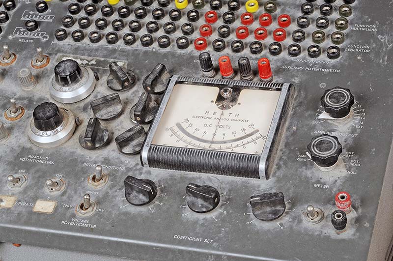
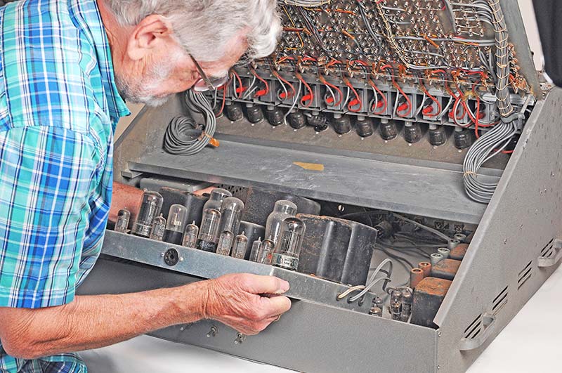
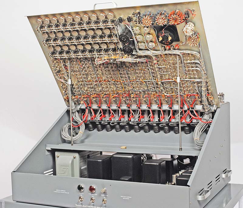
Fast forward six decades. Today, I finally have one in my shop on my bench completely restored! Figure 2 is the proof. It took me eight months of part-time work to restore all 168 pounds. In this article, I would like to share a few of the trials and tribulations I went through to resurrect this beast.
Several years ago, I restored Heathkit’s smaller analog computer, the EC-1. You may have read about it in the May 2016 issue of Nuts & Volts. Afterwards, I vowed to find and restore my dream computer: the ES-400. Amazingly, a nice gentleman in Northern California heard about my quest and just happened to have one in his storage locker. He said I was welcome to it for free if I would give it a good home.


SPECIFICATIONS

The “Big Kahuna” had 25 major assemblies containing a total of 73 vacuum tubes and the following specifications:

Model: ES-400 (sometimes called H-1)
Original Price: $945 (equivalent 2019 dollars = $8,175)
Time Period Sold: 1956-1962
Quantity Sold: Approximately 250-400
Weight: 168 pounds
Dissipation: 450 watts

Assemblies:

(1) ES-2 Amplifier Power Supply (regulated ±250V at 250 mA, -450V at 50 mA, 6.3VAC at 14.5A)
(1) ES-50 Reference Power Supply (regulated ±100V)
(3) ES-100 Initial Condition Power Supply (2x floating 100V, in each supply)
(1) ES-151 Relay Power Supply (2x 50V)
(15) ES-201 Operational Amplifier (gain = 50,000, output range ±100V at 10 mA)
(1) ES-400 Cabinet and Front Panel (364 jacks, 52 switches, 38 pots, 14 connectors, one meter)
(1) ES-505 Repetitive Oscillator (0.6-6 Hz)
(1) Sola Voltage Regulator Transformer (250 VA)
(1) ES-600 Function Generator (optional)


His restoration wasn't cheap. A few examples from the article:

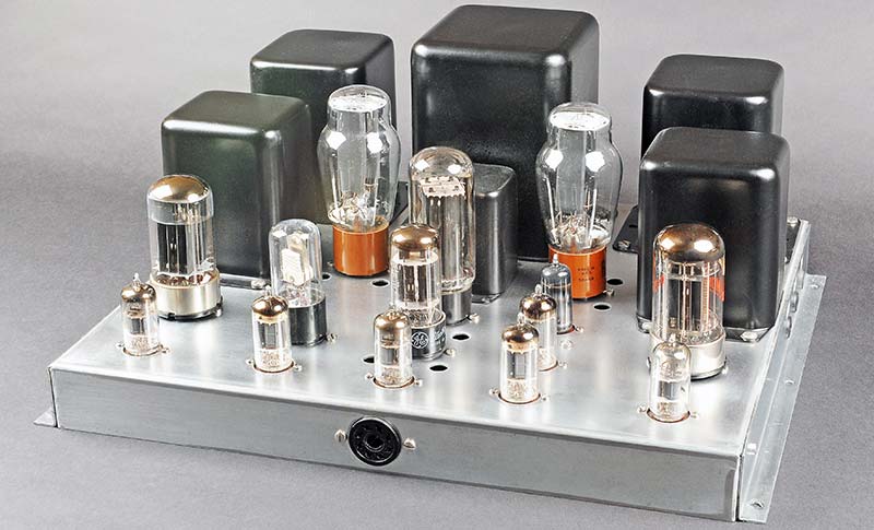
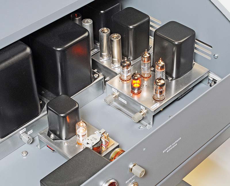
Problem: Unfortunately, the “free” computer did not include any of the 45 tubes for the 15 op-amps across the top of the cabinet. The 6BQ7As and 6BH6s were pretty reasonable, but the (15) 12AX7s were another story. Some eBay prices were pretty outrageous; $499.99 for a matched pair!!

Solution: Luckily, Chinese 12AX7A tubes were available from TubesAndMore.com for $9.59 each and they worked fine. Refer to Figure 14.

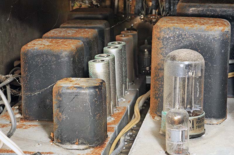
Problem: All the nuts and bolts were corroded, as were many other electrical components.

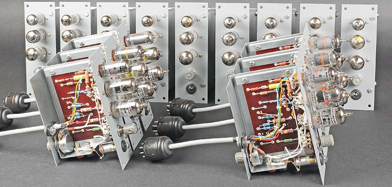
Solution: I replaced every nut, bolt, screw, and washer in the entire machine, and also 51 pots, 64 tube sockets, eight toggle switches, 15 octal plugs, and eight power cords. Plus, the countless resistors and capacitors. Whew!


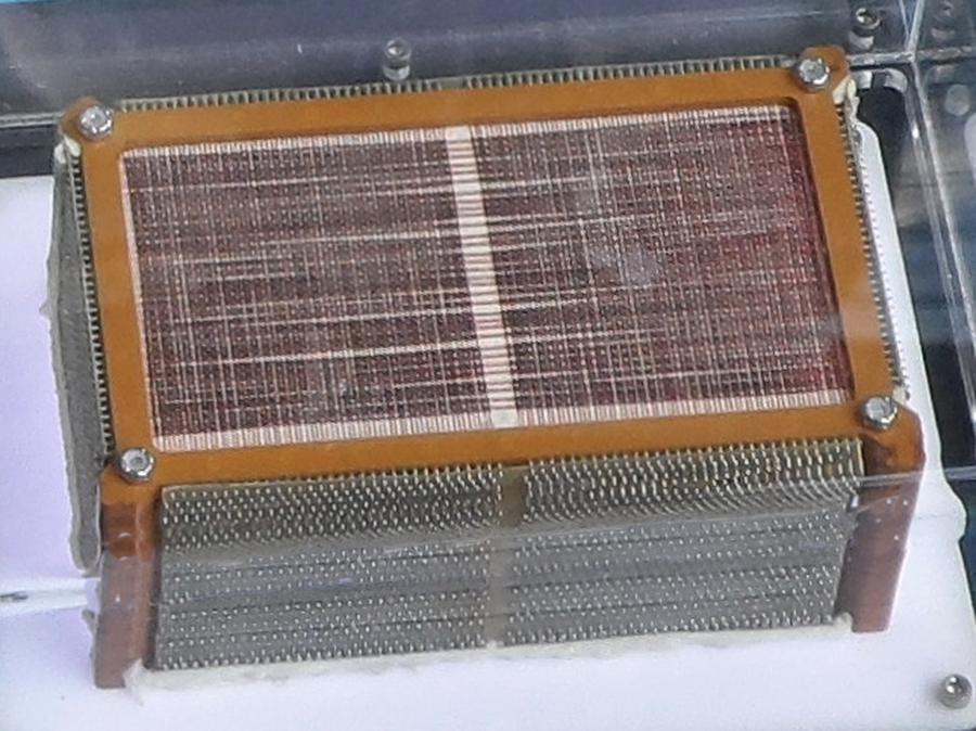
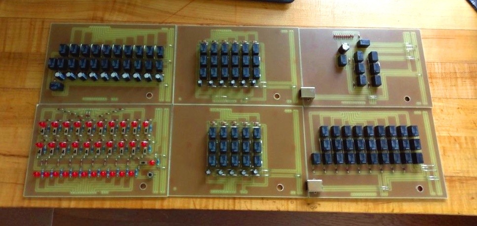
Just some of the photos from the article:
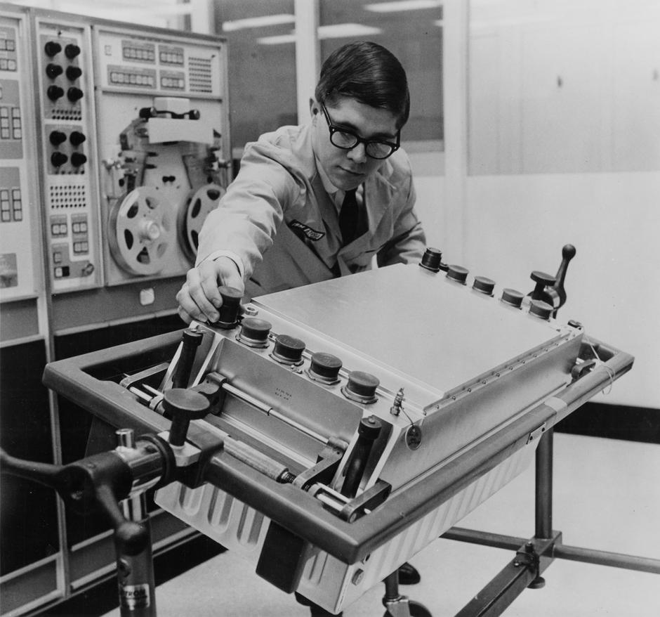
Before:

NV_0319_Goodsell_Figure03.jpg

NV_0319_Goodsell_Figure04.jpg

NV_0319_Goodsell_Figure05.jpg


After. Beautiful work:

NV_0319_Goodsell_Figure08.jpg

NV_0319_Goodsell_Figure15.jpg

NV_0319_Goodsell_Figure10.jpg

NV_0319_Goodsell_Figure13.jpg

NV_0319_Goodsell_Figure02.jpg
 
Amazing progress considering how incredibly difficult even 7nm is!

https://www.rocketryforum.com/threa...l-cool-electronics.133919/page-4#post-1781814

TSMC: 5nm on Track for Q2 2020 HVM, Will Ramp Faster Than 7nm
October 23, 2019

https://www.anandtech.com/show/15016/tsmc-5nm-on-track-for-q2-2020-hvm-will-ramp-faster-than-7nm

TSMC: 3nm EUV Development Progress Going Well, Early Customers Engaged
July 23, 2019

https://www.anandtech.com/show/1466...t-progress-going-well-early-customers-engaged

TSMC Starts $19.5 Billion 3nm Fab Construction
October 26, 2019

https://www.tomshardware.com/news/tsmc-fab-3nm-5nm-process-intel-samsung

tsmc_fab_14_fab14_semiconductor_chip_inside.jpg
 
Field Effect Transistor concept patent from 1930! How different history might have been if this had been seriously further researched at the time:

https://patentimages.storage.googleapis.com/fa/5d/33/ed2769d48fac4d/US1745175.pdf

Julius Edgar Lilienfeld

https://en.wikipedia.org/wiki/Julius_Edgar_Lilienfeld

Julius Edgar Lilienfeld (April 18, 1882 – August 28, 1963) was a Polish/American physicist and electrical engineer, credited with the first patents on the field-effect transistor (FET) (1925) and electrolytic capacitor (1931). Because of his failure to publish articles in learned journals and because high-purity semiconductor materials were not available yet [but could have been if his patent had been widely known and worked on - W], his FET patent never achieved fame, causing confusion for later inventors.
 
Very bizarre occurrence.

High Voltage Created From Falling Snow?

 
My Uncle was a TV repairman back during the vacuum tubes and analog components.

After he retired from the TV business I would tell him about the new advances in electronics
that had been made.

He was most amazed at the miniaturization of the transistor. 1 transistor was the size of a #2
pencil eraser back then and now that same space can have over a million + transistors on it

Bobby
 
I got my "start" by working for the local TV and appliance repair guy who just happened to be the best man for my parent's wedding as well as a good friend to them.
I used to sit for 3 or 4 hours after school testing tubes for him and helping clean up the store and work areas. He gave me a few old TV's that were not worth fixing up to him so I spent a lot of evenings in the basement of our house "tinkering" with them. I got 3 TV's to actually work pretty well, so I had one for my bedroom and gave the other two away to two of my friends.

My start in electronics was when I went into the Air Force and was repairing system components of a Flight Director System for the KC-135 aircraft that I worked on as an Instrument Technician in the 70's. Yea, the days of the eraser sized transistors was something. Along with capacitors that were the size of a soda can!

Today's electronics are nothing even close but the test gear is certainly a lot better now. Used to be a "close guess" when repairing some things as the oscilloscopes were pretty crude back then as well.
 
The core memory inside a Saturn V rocket's computer

https://www.righto.com/2020/03/the-core-memory-inside-saturn-v-rockets.html

The Launch Vehicle Digital Computer (LVDC) had a key role in the Apollo Moon mission, guiding and controlling the Saturn V rocket. Like most computers of the era, it used core memory, storing data in tiny magnetic cores. In this article, I take a close look at an LVDC core memory module from Steve Jurvetson's collection. This memory module was technologically advanced for the mid-1960s, using surface-mount components, hybrid modules, and flexible connectors that made it an order of magnitude smaller and lighter than mainframe core memories. Even so, this memory stored just 4096 words of 26 bits.

It's interesting to compare the size of the LVDC's core memory to IBM's commercial core memories, which I wrote about here. The 128-kilobyte expansion for the IBM S/360 Model 40 computer required an additional cabinet weighing 610 pounds and measuring 62.5"×26"×60". An LVDC core memory module holds 4K words of 26 bits, equivalent to 13 kilobytes. Doing the math, the LVDC has 1/12 the weight and 1/40 the volume per byte. The core stack itself was very similar between the LVDC and the S/360 machines; the difference in weight and volume comes from the surrounding electronics and packaging.


vintage-lvdc.jpg

iu-lvdc-memory-group-w500.jpg

lvdc-core-module.jpg

core-stack-w450.jpg
 
To skip most of the theory, start at 30:00.

The 10,000 Year Shift Register (pseudo-random number generator)
 
After an overview to describe the issues - a stupid Coleco design which requires an external Coleco printer to power the CPU unit and EMP from that printer's power supply erasing the proprietary, custom designed and formatted compact cassettes for the system - at 8:13 we see a super sped up board design process followed by PCB ordering and prototype assembly, testing and troubleshooting.

Making a New Coleco Adam Internal PSU
 
Just incredible. A human hair is approximately 60,000 nanometers wide.

TSMC Starts 2nm Process Development for Fast, Efficient Chips
24 Apr 2020

https://www.tomshardware.com/news/tsmc-2nm-process-development-cpus-5nm-processors
At the start of this year we heard that TSMC was investing heavily in 5nm fabrication, and it's no secret that the next step after that is TSMC's 3nm process.The Taiwanese silicon manufacturer is looking beyond that process too, as it just announced to shareholders that it is starting development of its 2nm lithographic process, as spotted by DigiTimes.

Painstakingly few details are available about the 2nm process. All we know is that TSMC is starting development -- though it's safe to assume the end product will be very fast and more efficient than anything on the market today.

Currently, TSMC's 7nm process is in its peak, receiving huge numbers of orders from AMD for its Ryzen 3000-series CPUs and Navi graphics cards. Other customers include Apple, and although Huawei was to be included, that doesn't appear to be working out so well.

On the 5nm front, TSMC is working with EUV lithography, similar to what Samsung is accomplishing. The two chipmakers are neck-in-neck in the silicon race. According to DigiTimes, TSMC is expecting 10% of this year's revenue to come from its 5nm EUV lines.

After that, the 3nm process will take over, and TSMC expects mass production to start in 2022.


TSMC Investing Heavily in 5nm Fabrication and Expanding 7nm Capacity
1 Jan 2020

https://www.tomshardware.com/news/t...in-5nm-fabrication-and-expanding-7nm-capacity
TSMC Starts $19.5 Billion 3nm Fab Construction
26 Oct 2019

https://www.tomshardware.com/news/tsmc-fab-3nm-5nm-process-intel-samsung
TSMC is currently working on getting its 5nm process node into volume production in the first half of 2020. In early 2018, TSMC broke ground on its Fab 18 for 5nm production. Fab 18 has a size of 42 hectares, 160,000 square meters of cleanroom area, and will have a capacity of over one million wafers per month when all three phases are completed in 2021, providing work for 4,000 people.

The reported 2023 schedule for 3nm volume production would be noteworthy as TSMC has opted for at most a two-year cadence for all of its nodes since 20nm in late 2014. In general, TSMC has opted for shrinks of at most 2x density scaling with a more steady cadence, while Intel introduced the term hyperscaling at 10nm to describe its ambitious 2.7x scaling on 10nm and 2.5x on 14nm.

Samsung plans to begin its own 3nm production in 2021, based on gate-all-around (GAA) technology, although its density will not be as high as TSMC’s 3nm. (For Samsung, 5nm is an optimization of its 7nm node.)
 
I retired from Intel in May 2015, and at that time the company was having challenges getting 10 nm up and running (solid yield). It has been almost five years, and they just began shipping mobile processors late last year. Mobile = low volume, and higher ASP. To me, that signals continued yield challenges. I wonder what has happened to Intel's ability to execute?!? At some point, it seems they may be forced to look at outsourcing their Fab efforts to some extent in order to remain a viable player in the processor market.
 
I retired from Intel in May 2015, and at that time the company was having challenges getting 10 nm up and running (solid yield). It has been almost five years, and they just began shipping mobile processors late last year. Mobile = low volume, and higher ASP. To me, that signals continued yield challenges. I wonder what has happened to Intel's ability to execute?!? At some point, it seems they may be forced to look at outsourcing their Fab efforts to some extent in order to remain a viable player in the processor market.

10 years ago or so I read where Intel, IBM, Microsoft, and other chip manufactures/computer industry companies rented the Dept of Energy Nuclear lab super computers to try to find a way around the quantum issues with going to smaller chips. I think the reason you've seen multiple cores in processors is because they haven't been able to get past the quantum physics of getting smaller. I suspect that going the wrong way on research 10 years ago my be coming back to haunt some of the chip makers today. Intel may be one of them.
 
10 years ago or so I read where Intel, IBM, Microsoft, and other chip manufactures/computer industry companies rented the Dept of Energy Nuclear lab super computers to try to find a way around the quantum issues with going to smaller chips. I think the reason you've seen multiple cores in processors is because they haven't been able to get past the quantum physics of getting smaller. I suspect that going the wrong way on research 10 years ago my be coming back to haunt some of the chip makers today. Intel may be one of them.
No idea... I’m not a device physicist. I knew quite a few of them at Intel, and all I can say is that this (whatever “THIS” is) must be a REALLY challenging problem!

I can absolutely attest that architectural enhancements are counted toward Moore’s law metrics. Scaling transistors is a (mostly) 2D resolution to the scaling problem. All the tricks in a vendor’s portfolio count toward the metric of 2x performance per year or two.
 
At some point, it seems they may be forced to look at outsourcing their Fab efforts to some extent in order to remain a viable player in the processor market.
That's what AMD did out of economic necessity and based upon what the TMSC fabs can do for them that turned out to be a really smart move.
 
I think the reason you've seen multiple cores in processors is because they haven't been able to get past the quantum physics of getting smaller.
Much earlier here I posted a detailed post about the insane difficulty in getting 7nm working. Although quantum effects are relevant, the primary reason AMD went to chiplets (and Intel now knows it needs to go there, too, and is working on it) is yield per wafer.

The larger a die is on the wafer, the more likely it is to contain a defect, destroying the return from that area of silicon. A smaller die will still contain that random defect, but will destroy a smaller area. Plus, when using a multi-die CPU method, the same basic CPU dies (I hate the official, proper term "dice") can be used to create multiple CPU versions for different price ranges, just adding or subtracting dies as needed. Even if they can eventually match the TMSC fab results, unless Intel moves away from large, monolithic CPU dies (and they plan to), they will never be able to match AMD on price/performance.
 
Common Sense Comes Closer to Computers
The problem of common-sense reasoning has plagued the field of artificial intelligence for over 50 years. Now a new approach, borrowing from two disparate lines of thinking, has made important progress.

https://www.quantamagazine.org/common-sense-comes-to-computers-20200430/
“The real world is really complicated,” Rajani said. “But natural language is like a low-dimensional proxy for how the real world works.”

US patent office rules that artificial intelligence cannot be a legal inventor
Only ‘natural persons’ need apply
Apr 29, 2020

https://www.theverge.com/2020/4/29/...patent-trademark-office-intellectual-property
 
That's what AMD did out of economic necessity and based upon what the TMSC fabs can do for them that turned out to be a really smart move.
Yes, I recall their divestiture of most fab assets to Global Foundries several years ago (I believe they maintained their development fabs, but have since lost track of what they do or do not have in their possession). That signaled to me that AMD was understandably not able to keep up with the Intel's fab behemoth, and had relegated themselves to generation -1 or even -2 fab processes... which meant commodity processors sold on cost rather than performance. That was, in fact how things played out until fairly recently. Intel has been sitting on 14 nm products for over 6 years, which is an eternity in the world of semiconductors.
 
Great video on the advantages of chiplets vs monolithic dies. Watch from 8:00:

An Epyc Master Plan
Feb 21, 2018

 
10 years ago or so I read where Intel, IBM, Microsoft, and other chip manufactures/computer industry companies rented the Dept of Energy Nuclear lab super computers to try to find a way around the quantum issues with going to smaller chips. I think the reason you've seen multiple cores in processors is because they haven't been able to get past the quantum physics of getting smaller. I suspect that going the wrong way on research 10 years ago my be coming back to haunt some of the chip makers today. Intel may be one of them.
The good news for them is that most modern computing processes are multi-threaded, so having a whole bunch of slower processor cores tends to win out over having a few really fast cores. This is especially true in database or file servers... I've always said that all computers wait at the same speed...
 
I have a couple of friends who up until recently worked at Cray in Chippewa Falls, WI. Early on Cray realized that they didn't need faster processors but a faster I/O system so the processors wouldn't need to wait for data. So they created a very fast I/O system. Silicon Graphics bought Cray mainly to get their hands on this I/O system. Recently Cray was bought by HPE.

Now that there are many mutli-core CPUs out there I think that again, the pipeline is the week link. If you are not wasting CPU cycles waiting for data you can do a lot of number crunching.
Yes, that's what at first hurt AMD's Infinity Fabric (now Infinity Architecture) chiplet based performance versus a monolithic die CPU, but they've been working on improving that and the huge price/performance advantage allowing more cores overcomes that in most cases even with their first generation CPUs.
 
AMD is set to become TSMC's biggest 7nm customer in 2020

https://www.techspot.com/news/83400-amd-set-become-tsmc-biggest-7nm-customer-2020.html
In the second half of 2020, AMD will double their 7nm orders making them TSMC’s largest customer of 7nm chips according to some forecasts. Going into 2020, TSMC's factories have the capacity to produce 110,000 WPM (wafers per month) of 7nm chips and by the end of the year, they’ll be making 140,000 WPM. AMD will be buying about 20% of that capacity, according to Apple Daily.

Presently, AMD doesn’t make it into the top five at the TSMC club. Apple is their largest 7nm customer but they are expected to move to the 5nm node for the A14 SoC, taking two-thirds of TSMC’s 5nm capacity.

[snip]

But that may also mean there’s not much room to expand in the desktop CPU market, so what’s AMD going to use all that 7nm fab space for? Consoles, possibly.

The PlayStation 5 is already confirmed to be using AMD’s 7nm Zen 2 and Navi, and the Xbox Series X is expected to do the same. Both will sell in outrageous volume, no doubt justifying AMD’s large purchase and making them a tidy profit.


A thing of beauty. It should be in the U.S., but at least it's in Taiwan and not the CCP's mainland China:

2020-01-04-image-3.jpg
 
Original Rare Apple 1 Computer Demo at Vintage Computer Festival VCF East

 
The A100 GPU has 54 billion transistors, 65.4 million transistors per square MILLIMETER. The RTX 2080 Ti high end consumer graphics card costing $1,300 has 18.6 billion transistors. A Ryzen 9 3900X CPU has 3.8 billion transistors. A100 is not a product for general consumers at an estimated $20,000.

NVIDIA's massive A100 GPU isn't for you


NVIDIA Ampere A100 ‘Worlds Biggest 7nm GPU’ Official – Full Architecture


NVIDIA-GA100-GPU-Ampere.jpg


nvidia-ampere-ga100-full-gpu-architecture.jpg

In highly technical vernacular, that would be considered "a beast". :)
 
Back
Top