Not for rocketry, but still cool electronics

The Rocketry Forum

Help Support The Rocketry Forum:

This site may earn a commission from merchant affiliate links, including eBay, Amazon, and others.
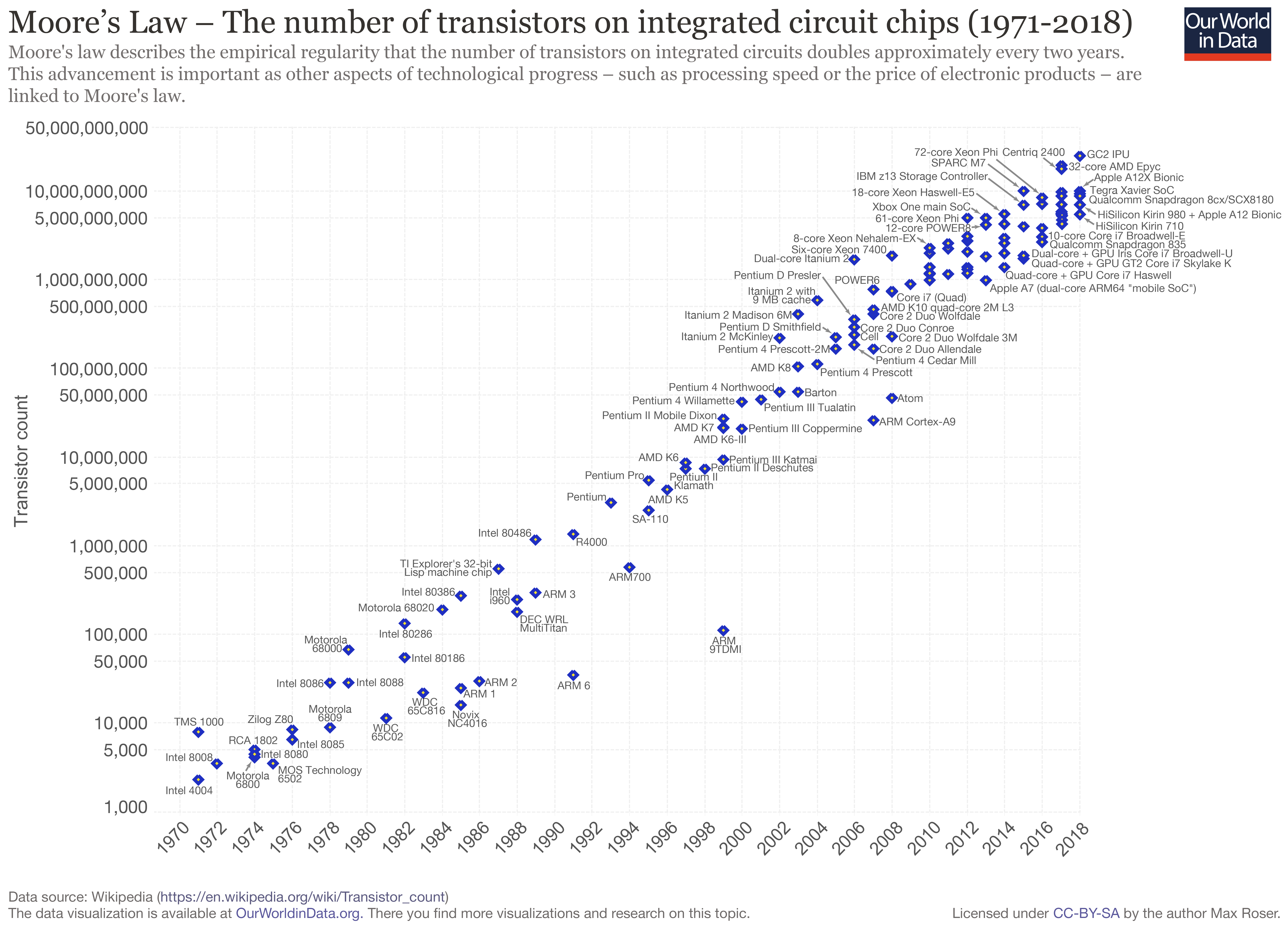
Intel sees the light and admits without explicitly saying so that some sort of multi-chip architecture like AMD's Infinity Fabric is the way to go. They will not be able to compete with AMD on price/performance until they split their large, lower yield, and therefore much more expensive monolithic CPU dies into multiple, interconnected, smaller dies.

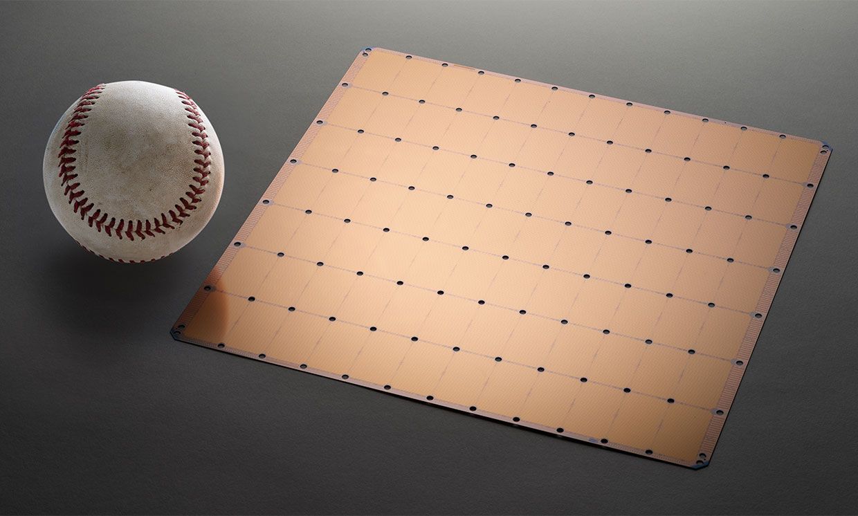
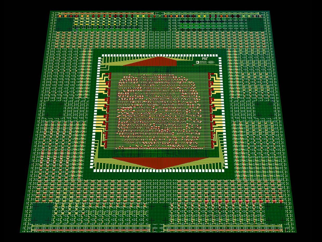
Intel's View of the Chiplet Revolution
Ramune Nagisetty is helping Intel establish its place in a new industry ecosystem centered on chiplets

https://spectrum.ieee.org/tech-talk/semiconductors/processors/intels-view-of-the-chiplet-revolution


frontier_amd_supercomputer_DOE_cray.jpg
 
As I've said here before ( https://www.rocketryforum.com/threa...l-cool-electronics.133919/page-6#post-1877202 ), until Intel manages to come up with their own version of AMD's Infinity Fabric architecture to allow their huge monolithic and, therefore, much lower yield and, therefore, expensive CPUs to be reduced to interconnected much smaller, much higher production yield dies, they are toast in the price/performance race with AMD. AMD is now attacking them hard in ALL of Intel's still unjustifiably dominated markets.

AMD Ryzen 3000 Announced: Five CPUs, 12 Core CPU for $499 [which beats $1100 Intel CPU performance - W], up to 4.6 GHz, PCIe 4.0, [IPC now equal to or better than Intel's, all at incredibly low TDPs (power) due to 7nm process - W], coming on 7/7/19
May 26, 2019

https://www.anandtech.com/show/1440...-cores-for-499-up-to-46-ghz-pcie-40-coming-77


Years ago I followed CPU news in great detail, but lost interest when Intel became a virtual monopoly. I could kick myself that I wasn't paying attention - AMD $1.67 per share in 2015, $26.40 per share now, four years later. From an Intel fanboy often sponsored by Intel:

 
Last edited:
In his annual Maker Faire Bay Area presentation, Arduino co-founder Massimo Banzi reveals the new Arduino Nano boards, new open-source community support, and professional-grade updates to a new Arduino IDE.

 
PCBWay's factory:


JLPCB's factory tour I've previously posted:

 
The T-800 Terminator model used a ultra-ultra-super-duper MOS6502 compatible CPU running Apple II magazine software. ;) I recognized that it was assembly language code, but didn't know it was 6502.

"My CPU is a neural-net processor; a learning computer." - T-800 - Terminator 2: Judgment Day

The 6502 in "The Terminator"

https://www.pagetable.com/?p=64

In the first Terminator movie, the audience sees the world from the T-800’s view several times. It is well-known that in two instances, there is 6502 assembly code on the T-800’s HUD, and many sites have analyzed the contents: It’s Apple-II code taken from Nibble Magazine. Here are HD versions of the shots, thanks to Dominik Wagner.

[one of the images at that link]

00-37-23.jpg
 
6 Things to Know About the Biggest Chip Ever Built
Startup Cerebras has built a wafer-size chip for AI
21 Aug 2019

https://spectrum.ieee.org/tech-talk...ngs-to-know-about-the-biggest-chip-ever-built

On Monday at the IEEE Hot Chips symposium at Stanford University, startup Cerebras unveiled the largest chip ever built. It is roughly a silicon wafer-size system meant to reduce AI training time from months to minutes. It is the first commercial attempt at a wafer-scale processor since Trilogy Systems failed at the task in the 1980s.

1 | The stats

As the largest chip ever built, Cerebras’s Wafer Scale Engine (WSE) naturally comes with a bunch of superlatives. Here they are with a bit of context where possible:

Size: 46,225 square millimeters. That’s about 75 percent of a sheet of letter-size paper, but 56 times as large as the biggest GPU.
Transistors: 1.2 trillion. Nvidia’s GV100 Volta packs in 2.1 billion.
Processor cores: 400,000. Not to pick on the GV100 too much, but it has 5,660.
Memory: 18 gigabytes of on-chip SRAM, about 3,000 times as much as our pal the GV100.
Memory bandwidth: 9 petabytes per second. That’s 10,000 times our favorite GPU, according to Cerebras.

2 | Why do you need this monster?

Cerebras makes a pretty good case in its white paper [PDF] for why such a ridiculously large chip makes sense. Basically, the company argues that the demand for training deep learning systems and other AI systems is getting out of hand. The company says that training a new model—creating a system that, once trained, can recognize people or win a game of Go—is taking weeks or months and costing hundreds of thousands of dollars of compute time. That cost means there’s little room for experimentation, and that’s stifling new ideas and innovation.

3 | What’s in those 400,000 cores?

According to the company, the WSE’s cores are specialized to do AI, but still programmable enough that they’re not locked into only one flavor of it. They call them Sparse Linear Algebra (SLA) cores. These processing units are specialized to “tensor” operations key to AI work, but they also include a feature that reduces the work, particularly for deep-learning networks. According to the company, 50 to 98 percent of all the data in a deep learning training set are zeros. The nonzero data is therefore “sparse.”

4 | How did they do this?

The fundamental idea behind Cerebras’s massive single chip has been obvious for decades, but it has also been impractical.
The most basic problem is that the bigger the chip, the worse the yield; that’s the fraction of working chips you get from each wafer. Logically, this should mean a wafer-scale chip would be unprofitable, because there would always be flaws in your product. Cerebras’s solution is to add a certain amount of redundancy. According to EE Times, the Swarm communications networks have redundant links to route around damaged cores, and about 1 percent of the cores are spares.


Startup Spins Whole Wafer for AI
Cerebras taps wafer-scale integration for training
19 Aug 2019

https://www.eetimes.com/document.asp?doc_id=1335043&page_number=1

Startup Cerebras will describe at Hot Chips the world’s largest semiconductor device, a 16nm wafer-sized processor array that aims to unseat Nvidia’s GPUs dominance in training neural networks. The whopping 46,225mm2 die consumes 15kW, packs 400,000 cores, and is running in a handful of systems with at least one unnamed customer.

The company will not comment on the frequency of the device which is likely low to help manage its power and thermal demands. The startup’s veteran engineers have “done 2-3 GHz chips before but that’s not the goal here--the returns to cranking the clock are less than adding cores,” said Andrew Feldman, chief executive and a founder of Cerebras.

Feldman wouldn’t comment on the cost, design or roadmap for the rack system Cerebras plans to sell. But he said the box will deliver the performance of a farm of a thousand Nvidia GPUs that can take months to assemble while requiring just 2-3% of its space and power.


The five technical challenges Cerebras overcame in building the first trillion-transistor chip
19 Aug 2019

https://techcrunch.com/2019/08/19/t...-building-the-first-trillion-transistor-chip/

MzM1OTIwNw.jpeg
 
A Carbon Nanotube Microprocessor Mature Enough to Say Hello
Three new breakthroughs make commercial nanotube processors possible
28 Aug 2019

https://spectrum.ieee.org/nanoclast...n-microprocessor-built-using-carbon-nanotubes

Engineers at MIT and Analog Devices have created the first fully-programmable 16-bit carbon nanotube microprocessor. It’s the most complex integration of carbon nanotube-based CMOS logic so far, with nearly 15,000 transistors, and it was done using technologies that have already been proven to work in a commercial chip-manufacturing facility. The processor, called RV16X-NANO, is a milestone in the development of beyond-silicon technologies, its inventors say.

Unlike silicon transistors, nanotube devices can easily be made in multiple layers with dense 3D interconnections. The Defense Advanced Research Projects Agency is hoping this 3D aspect will lead to commercial carbon nanotube (CNT) chips with the performance of today’s cutting-edge silicon but without the high design and manufacturing cost.


MzM2Mjc3OA.jpeg
 
Unix at 50: How the OS that powers smartphones started from failure
Today, Unix powers iOS and Android
29 Aug 2019

https://arstechnica.com/gadgets/201...rame-a-gator-and-three-dedicated-researchers/

Excerpts from LONG article:

Multics had started off hopefully enough, although even at first glance its goals were a bit vaguely stated and somewhat extravagant.

A collaboration involving GE, MIT, and Bell Labs, Multics was promoted as a project that would turn computing power into something as easy to access as electricity or phone service.

[Multics project failed]

Baker and Davis had initially taken away the Multics project without giving McIlroy’s team something new to work on, and this caused a fair bit of apprehension for the programmers on McIllroy’s team. They worried that their positions at Bell Labs would not long survive the demise of Multics.

However, this burgeoning development team happened to be in precisely the right environment for Unix to flourish. Bell Labs, which was funded by a portion of the monthly revenue from nearly every phone line in the United States, was not like other workplaces. Keeping a handful of programmers squirreled away on the top floor of the Murray Hill complex was not going to bankrupt the company. Thompson and co. also had an ideal manager to pursue their curiosity. Sam Morgan, who managed the Computing Science Research Department (which consisted of McIlroy’s programmers and a group of mathematicians), was not going to lean on McIlroy’s team because they suddenly had nothing in particular to work on.

Still, there was one tiny problem for Thompson and his fellow tinkerers at the moment—nobody had a computer. While lab management had no problem with computers as such, McIlroy’s programmers couldn’t convince their bosses to give them one. Having been burned badly by the Multics fiasco, Davis wasn’t sold on the team’s pitch to give them a new computer so they could continue operating system research and development. From lab management’s perspective, it seemed like Thompson and the rest of the team just wanted to keep working on the Multics project.

And in a situation seemingly calculated to irritate Ritchie and Thompson—who each already nursed a certain disdain for corporate bureaucracy—the acoustics department had no shortage of computers. In fact, acoustics had more computers than they needed. When that department’s programs grew too complicated to run efficiently on the computers they had, they simply asked labs management for new computers and got them.

With the rest of the team’s help, Thompson bundled up the various pieces of the PDP-7—a machine about the size of a refrigerator, not counting the terminal—moved it into a closet assigned to the acoustics department, and got it up and running. One way or another, they convinced acoustics to provide space for the computer and also to pay for the not infrequent repairs to it out of that department’s budget.

McIlroy’s programmers suddenly had a computer, kind of. So during the summer of 1969, Thompson, Ritchie, and Canaday hashed out the basics of a file manager that would run on the PDP-7.

Although the labs didn’t keep a close eye on when its researchers arrived at work—or when they left—Canaday did his best to keep normal business hours that summer. Thompson and Ritchie, however, were a bit more relaxed.

Both of them kept wildly irregular hours. Thompson told the Unix Oral history project he was working on about a 27-hour day at the time, and that put him out of sync with everyone else’s 24-hour day. Ritchie was just a traditional night owl. So the earliest these three developers got together most days was over lunch, and even at that, there were occasions where Canaday found himself calling Thompson and Ritchie at their homes to remind them when the Bell Labs cafeteria closed.

In the cafeteria, the three developers hashed out the fundamentals of the file manager for this new operating system, paying little to no attention to the staff cleaning up the lunch mess around them. They also worked on the system in their offices up in the computer science department. McIlroy, who had the office across the hall from Canaday, remembered them working around a blackboard that summer.

Eventually when they had the file management system more or less fleshed out conceptually, it came time to actually write the code. The trio—all of whom had terrible handwriting—decided to use the Labs’ dictating service. One of them called up a lab extension and dictated the entire code base into a tape recorder. And thus, some unidentified clerical worker or workers soon had the unenviable task of trying to convert that into a typewritten document.
Of course, it was done imperfectly. Among various errors, “inode” came back as “eye node,” but the output was still viewed as a decided improvement over their assorted scribbles.

In August 1969, Thompson’s wife and son went on a three-week vacation to see her family out in Berkeley, and Thompson decided to spend that time writing an assembler, a file editor, and a kernel to manage the PDP-7 processor. This would turn the group’s file manager into a full-fledged operating system. He generously allocated himself one week for each task.

Thompson finished his tasks more or less on schedule. And by September, the computer science department at Bell Labs had an operating system running on a PDP-7—and it wasn’t Multics.

Still, the team felt this was an accomplishment and christened their operating system “UNICS,” short for UNIplexed Information and Computing System. (At least, that’s the official explanation. According to Multics' history site, multicians.org, the pronunciation, like “eunuchs,” was considered doubly appropriate because the team viewed this new operating system, running on an obsolete hand-me-down computer, as “Multics without any balls.”)

The computer science department pitched lab management on the purchase of a DEC PDP-11 for document production purposes, and Max Mathews offered to pay for the machine out of the acoustics department budget. Finally, management gave in and purchased a computer for the Unix team to play with. Eventually, word leaked out about this operating system, and businesses and institutions with PDP-11s began contacting Bell Labs about their new operating system. The Labs made it available for free—requesting only the cost of postage and media from anyone who wanted a copy.

The rest has quite literally made tech history. By the late 1970s, a copy of the operating system found its way out to the University of California at Berkeley, and in the early 1980s, programmers there adapted it to run on PCs. Their version of Unix, the Berkeley Software Distribution (BSD), was picked up by developers at NeXT, the company Steve Jobs founded after leaving Apple in 1985. When Apple purchased NeXT in 1996, BSD became the starting point for OS X and iOS.

The free distribution of Unix stopped in 1984, when the government broke up AT&T and an earlier settlement agreement that prohibited the company from profiting off many Bell Labs inventions expired. The Unix community had become accustomed to free software, however, so upon learning that AT&T would soon be charging for all copies of Unix and would prohibit alterations to the source code, Richard Stallman and others set about re-creating Unix using software that would be distributed to anyone free of charge—with no restrictions on modification. They called their project “GNU,” short for “GNU’s Not Unix.” In 1991, Linus Torvalds, a university student in Helsinki, Finland, used several of the GNU tools to write an operating system kernel that would run on PCs. And his software, eventually called Linux, became the basis of the Android operating system in 2004.
 
Commander X16 - modern 8-bit retro computer project

Very clever retro-hardware architecture using old IC types still in production, but they already have a decent emulator to aid hardware development which will only get better with time. Some people simply must have hardware but, for instance, as an Amiga expert/fanatic on YouTube has demonstrated and admitted, the fastest, cheapest by far, and most convenient (USB I/O, HDMI out, etc.) Amiga system is one emulated on a Raspberry Pi.


Emulator:

https://github.com/commanderx16/x16-emulator/releases
 
John Carmack: Circumventing Moore's Law
28 Aug 2019

John D. Carmack II (born August 20, 1970) is an American computer programmer, video game developer and engineer. He co-founded id Software and was the lead programmer of its video games Commander Keen, Wolfenstein 3D, Doom, Quake, Rage and their sequels. Carmack made innovations in 3D graphics, such as his Carmack's Reverse algorithm for shadow volumes.

 
Ah memories... I built a 4-bit CPU out of 7400's back in the mid 70's. Four perfboards, programmed with switches and a "deposit" button. Later on when I got a job working with PDP-11's, that experience came in handy... I often had to bootload it with switches.
 
In the '70's at Hughes Aircraft we were making signal processors with bit-slice chips. That was where the components of the processor were implemented in 4 or 8-bit chip 'slices' that you could stack together to build a custom word-length processor. I'll never forget that the 'bible' for bit-slice design was Mick & Brick "Bit-Slice Microprocessor Design". (May still have that here somewhere.) That signal processor was used in the ADCAP-48 torpedo, AN/BQQ5 sonar, and SURTASS towed sonar array. The group had t-shirts made with a picture of the processor on the front saying "One great success..." and the back said "...after another." with a picture of the Spruce Goose.
 
Last edited:
Later on when I got a job working with PDP-11's, that experience came in handy... I often had to bootload it with switches.

I was programmer and system analyst for the computer system that runs Melbourne's (Australia) trains from '92-'98. All PDP11 units. They still use the same software, but the PDP11 processors are emulated by PCBs fitted with IBM Power PC cores. The reliability nowadays is much better. Still the piano-keys to plug the bootstrap codes in...
 
Homemade Silicon ICs / Computer Chips

Sam Zeloof
(my previous post about his efforts somewhere above)

https://en.wikipedia.org/wiki/Sam_Zeloof

Sam Zeloof (born 1999 or 2000) is an American autodidact who at the age of 17 constructed a home microchip fabrication facility in his garage[1]. In 2018 he produced the first homebrew lithographically fabricated microchip, the Zeloof Z1[2], a PMOS dual differential amplifier chip[3]. His work takes inspiration from Jeri Ellsworth's 'Cooking with Jeri' which demonstrates a homebrew transistor and logic gate fabrication process[4].


https://www.youtube.com/user/szeloof/videos

His blog:

https://sam.zeloof.xyz/first-ic/
 
I was programmer and system analyst for the computer system that runs Melbourne's (Australia) trains from '92-'98. All PDP11 units. They still use the same software, but the PDP11 processors are emulated by PCBs fitted with IBM Power PC cores. The reliability nowadays is much better. Still the piano-keys to plug the bootstrap codes in...
Cool. Love the emulation part. I've read that software from ANCIENT IBM mainframes are still being run... on emulators.

My PDP-11 CPU on a chip IC and die macro photos:

https://www.rocketryforum.com/threa...l-cool-electronics.133919/page-5#post-1824461
 
In the '70's at Hughes Aircraft we were making signal processors with bit-slice chips. That was where the components of the processor were implemented in 4 or 8-bit chip 'slices' that you could stack together to build a custom word-length processor. I'll never forget that the 'bible' for bit-slice design was Mick & Brick "Bit-Slice Microprocessor Design". (May still have that here somewhere.) That signal processor was used in the ADCAP-48 torpedo, AN/BQQ5 sonar, and SURTASS towed sonar array. The group had t-shirts made with a picture of the processor on the front saying "One great success..." and the back said "...after another." with a picture of the Spruce Goose.
Cool. I didn't have anything to do with their design and never programmed one, but I photographed some of their silicon dies:

AMD Am2903ADC Bit Slice CPU
IDT 49C402-BG84 Bit Slice CPU
Signetics N3002I Bipolar Bit Slice Processor
Texas Instruments SN74ACT8832AGB 32bit Bit-Slice Processor

The list of what I macro-photographed before I got bored:

45457509121_ac872c0e20_o.jpg
 
Today, 10/18, is Exascale Day. Note the mention of how very useful this will be for nuclear weapons "stockpile stewardship."

 
The Extreme Physics Pushing Moore’s Law to the Next Level

Awesome hardware shown.

 
The humble mineral that transformed the world

https://www.bbc.com/future/bespoke/made-on-earth/how-the-chip-changed-everything/

High-end electronics require high-quality ingredients. The purest silicon is found in quartz rock and the purest quartz in the world comes from a quarry near Spruce Pine in North Carolina, US. Millions of the digital devices around the world – perhaps even the phone in your hand or the laptop in front of you – carry a piece of this small North Carolina town inside them. “It does boggle the mind a bit to consider that inside nearly every cell phone and computer chip you’ll find quartz from Spruce Pine,” says Rolf Pippert, mine manager at Quartz Corp, a leading supplier of high-quality quartz.

The rocks around Spruce Pine are unique. High in silica, a silicon-containing compound, and low in contaminates, the region has been mined for centuries for gemstones and mica, a silicate used in paint. But the unearthed quartz was discarded. Then came the rise of the semiconductor industry in the 1980s and quartz turned into white gold.

Now, it sells for $10,000 (£8,250) a tonne, making the Spruce Pine mine a $300m-a-year operation. Rocks extracted from the ground with machines and explosives are put into a crusher, which spits out quartz gravel. This then goes to a processing plant, where the quartz is ground down to a fine sand. Water and chemicals are added to separate the silicon from other minerals. The silicon goes through a final milling before being bagged up and sent as a powder to a refinery.

For all the many billions of microchips in the world, only around 30,000 tonnes of silicon is mined each year. That’s less than the amount of construction sand produced each hour in the US alone. “The reserves here in the Spruce Pine area are very strong,” says Pippert. “We have decades of material. The industry will probably change before we run out of quartz.”
 
Countdown to Singularity


Moore%27s_Law_Transistor_Count_1971-2018.png


MooresLaw2.png


ELON MUSK’S BILLION-DOLLAR CRUSADE TO STOP THE A.I. APOCALYPSE
Elon Musk is famous for his futuristic gambles, but Silicon Valley’s latest rush to embrace artificial intelligence scares him. And he thinks you should be frightened too. Inside his efforts to influence the rapidly advancing field and its proponents, and to save humanity from machine-learning overlords.
MARCH 26, 2017

https://www.vanityfair.com/news/2017/03/elon-musk-billion-dollar-crusade-to-stop-ai-space-x
 
Birth of BASIC (Beginner's All-Purpose Symbolic Instruction Code)

 
I first used Basic on a Navy Snap II mini computer system from a terminal. Then it was on to the built-in Basic on the Tandy Color Computer II. I ended up learning assembler on the TCCII because the compiler was so slow. GW Basic on a pc and then QBasic. The best was QuickBasic because of the power and the fact the programs could be compiled to .exe files.

When I moved to MS Visual Basic for Applications in MS Access 2.0 it took me a little while to adapt to an event driven language rather than the sequential programming model used by all the earlier Basic programs.

It's amazing how Basic has evolved and is going strong today.
 
Back to his usual subject, the restoration of old mainframes, a video by one of the Apollo AGC restoration team members:

1958(!) FACOM 128B Japanese Relay Computer, still working!

 
THE BIZEN TRANSISTOR
https://hackaday.com/2019/11/23/new-part-day-the-bizen-transistor/

If we had a dollar for every exciting new device that’s promised to change everything but we never hear of beyond the initial hoopla, we’d own our own private islands in the sun from the beaches of which we’d pick out Hackaday stories with diamond-encrusted keyboards. The electronic engineering press likes to talk about new developments, and research scientists like a bit of publicity to help them win their next grant.

The Bizen transistor however sounds as though it might have some promise. It’s a novel device which resembles a bipolar transistor in which the junctions exhibit Zener diode-like properties, and in which the mechanism is through quantum tunneling rather than more conventional means. If this wasn’t enough, its construction is significantly simpler than conventional semiconductors, requiring many fewer support components to make a logic gate than traditional CMOS or TTL, and requires only eight mask steps to manufacture. This means that lead times are slashed, and that the cost of producing devices is much reduced.

The device’s originator has partnered with a semiconductor fab house to offer a service in which custom logic chips can be produced using the new devices in a series of standard building blocks. This is likely to be only of academic interest to the hacker at the moment, however the prospect of this cost reducing as the technology matures does show promise of reaching the means of some more well-funded hacker projects. It will be a while before we can order a chip with the same ease as a PCB, but this makes that prospect seem just a little bit closer.


Bipolar-Zener Combo Takes On CMOS
18 Oct 2019

https://www.eetimes.com/document.asp?doc_id=1335216#
 
Back
Top