Hall effect switch for Mini MOSFET Slide Switch with Reverse Voltage Protection

The Rocketry Forum

Help Support The Rocketry Forum:

This site may earn a commission from merchant affiliate links, including eBay, Amazon, and others.

roboticsmick

Member
Joined
Aug 21, 2022
Messages
5
Reaction score
1
Location
Australia
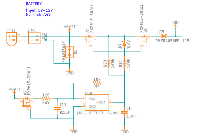
Hi all, I am trying my hand at designing a hall effect switch with reverse voltage protection that is always OFF by default.

hall-effect-switch.png


Does anyone have any suggestions or feedback for how I can improve and simply my design?

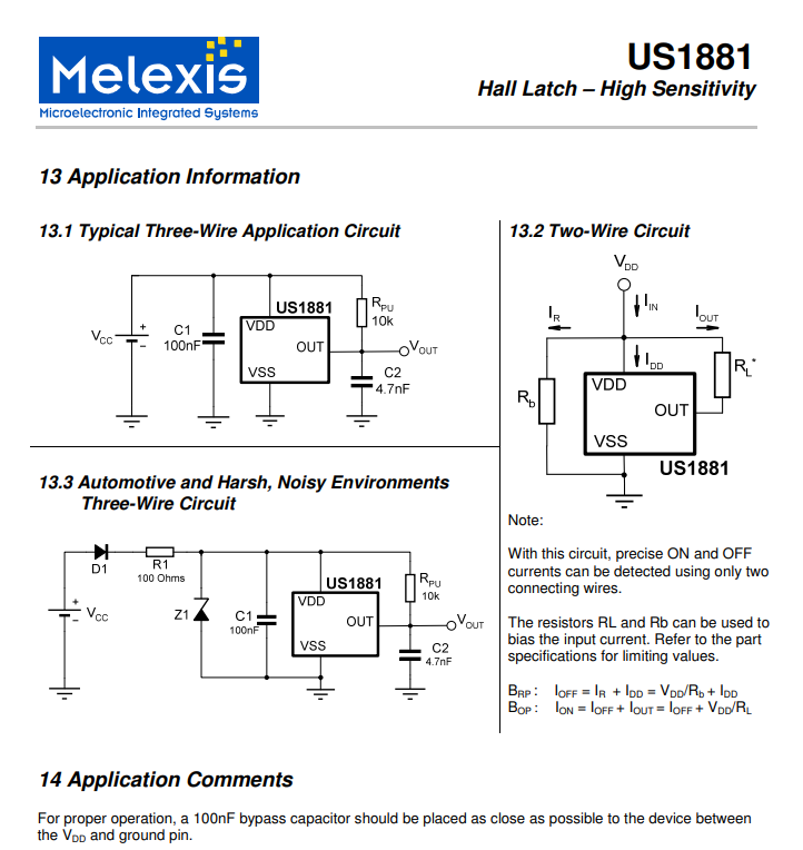
I’m using the US1881 latching hall effect sensor, but it needs it’s own reverse polarity protection circuit.

US1881.png


I'm basing the switch of Pololu's Mini MOSFET Slide Switch.

Thanks in advance for any advice!
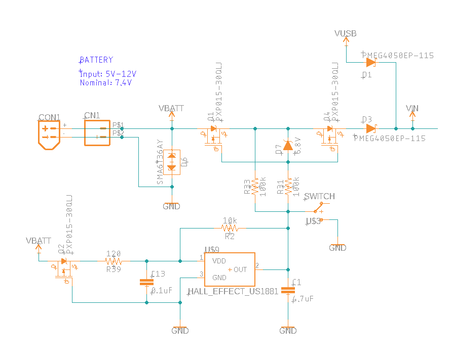
 
From a rocketry perspective, it's important that the circuit starts up in the OFF state. Also that any power glitch does not cause a full reset back to OFF. (switching flight electronics off mid flight is a bad idea.) On top of that the hall switch has to ONLY switch with a deliberate magnetic action, not an accidental one.
So you need to make sure you have a power up reset function and that in a reset state, it's off. My only concern would be the 4.7uF capacitor would be low at power up giving a low signal initially to the P-Mosfet and turning it on at startup.
Your circuit diagram shows a 4.7uF
The sample diagram shows a 4.7nF
Norm
 
I haven't gone through in detail, but I did spot that the 4u7 cap (C1) on the output of the hall switch was actually 4n7 in the application notes.

[edit] I also suspect you have your MOSFETs back to front if current is meant to be switched from the battery on the left to the load on the right. As it stands the body diodes will be forward-biased and just let the current through.
Yeah, you're correct, that second mosfet needs to be flipped. I was very confused when my first test board switch didn't work. I've corrected the second mosfet and capacitor value.
I've currently got it hooked up to an LED though, and sometimes I notice a small LED flash on startup when I first power the board. I'm a bit disappointed with the design. Mostly because I think my grasp of the correct logic for all the gates is clearly off. Making sure it's off by default, but also making sure it doesn't turn on with reverse polarity protection o_O

hallswitch.png
 
It's not as easy as some think to get a circuit into the correct state at power up every time.
If you use a Phliips 4017 it powers up with output 0 on every time. Use a Motorolla 4017 and it's a lucky dip for the 10 outputs unless you implement secondary logic to guarantee reset is held low /high for a period of time. Even different manufacturers of the same component have differences not always obvious unless you read the full spec.
Try connecting c1(gnd) to +v instead and fit a 1M pullup from U$9/2 to V bat and test to see what you get on startup. Then test operation.
Fix the FET too.
 
Yeah, you're correct, that second mosfet needs to be flipped. I was very confused when my first test board switch didn't work. I've corrected the second mosfet and capacitor value.
I've currently got it hooked up to an LED though, and sometimes I notice a small LED flash on startup when I first power the board. I'm a bit disappointed with the design. Mostly because I think my grasp of the correct logic for all the gates is clearly off. Making sure it's off by default, but also making sure it doesn't turn on with reverse polarity protection o_O

hallswitch.png

Remove R2 and see if it still flashes. R2 will cause your FETs to glitch on on power-up because C13 is not charged yet. It's also not needed because of R33.

There are some ways how you can simplify your design. Q1 is not needed, because of D3. If you move D3 before Vbatt, you can also get rid of Q2. The maximum Vgs of the PXP015 is 25V, so D7 it's not needed if you plan to only operate it up to 12V. You can reduce the voltage of your TVS a bit too, than it will protect the gate of Q4. If you remove D7, the functionality of R31 and R33 can also be handled by a single resistor from gate to source.

Reinhard
 
Back
Top